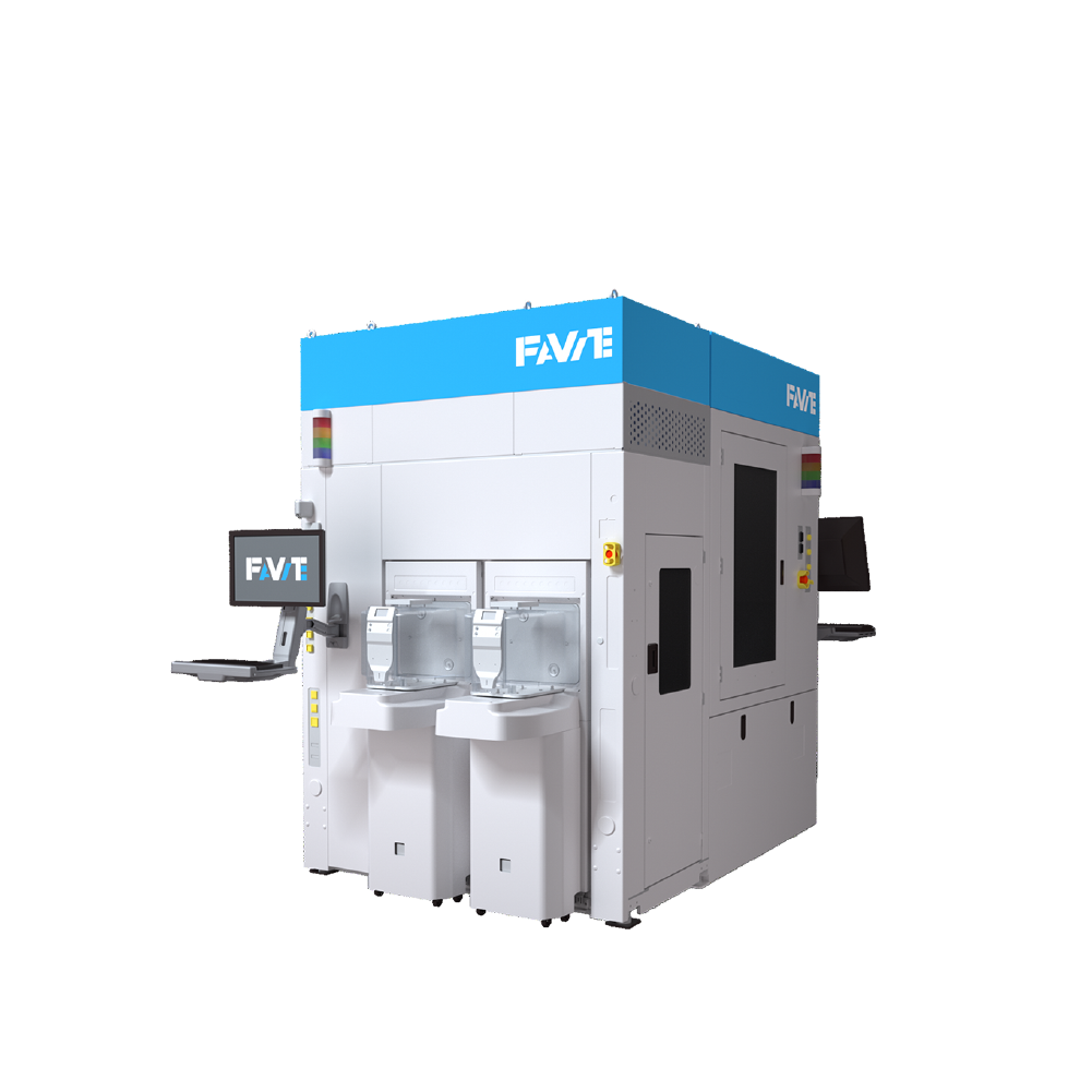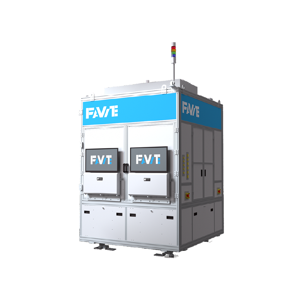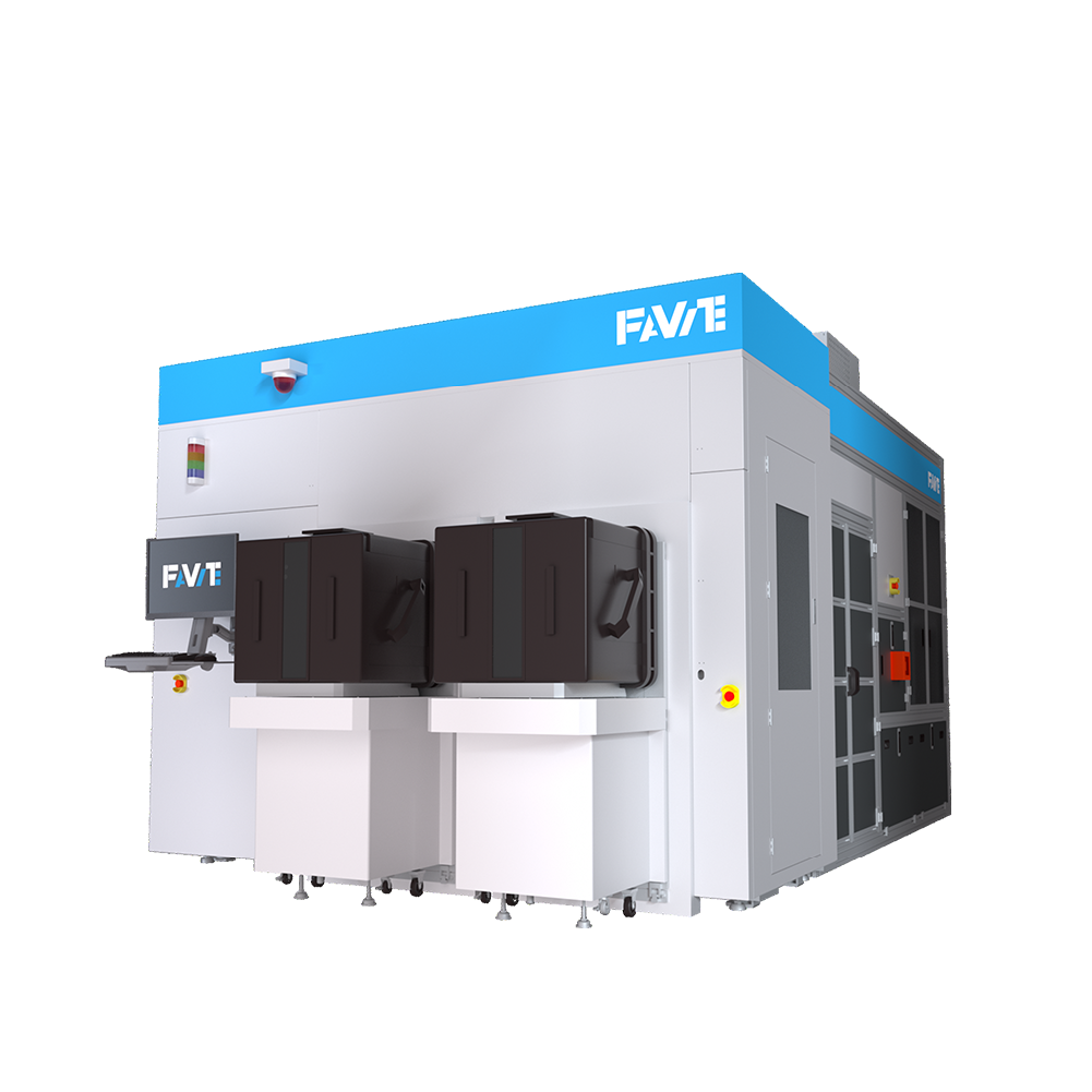
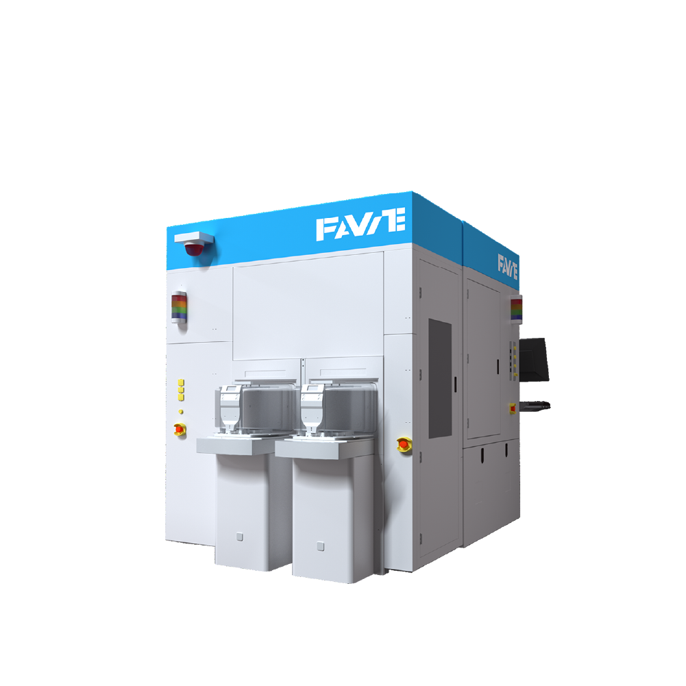
Horus A Series – FOWLP 3D IC High-Precision Die Shift Metrology Tool
Wafer Level 3D IC Package Die Location Metrology Tool
✔Applied for 3D IC advanced package
✔Support SoC die-to-wafer bonding process
✔Die shift/rotation feedback for hybrid bonding accuracy
Share: