Array AOI
✔ Resolution and defect detection capabilities ranging from 1μm~5μm
✔ Compatible with substrate sizes from G3.5 to G10.5
✔ Zero dead zone detection, achieving 100% coverage of the entire panel area
✔ Superior proprietary image inspection technology supporting all sizes, various pattern designs, and arbitrarily shaped panel products
✔ Intelligent defect classification functionality
✔ Professional and customized services available
Share:
Applied Field
LCD Panel Array Process
OLED Panel Array Process
Other Display Product Array Process
Features
In display panel manufacturing, Thin-Film Transistors (TFTs) act as switches controlling individual pixels and are arranged in an array configuration. Any defects within this array will directly impact the quality of the final product. The array process is susceptible to defects such as open circuits, short circuits, foreign material contamination, and Mura.
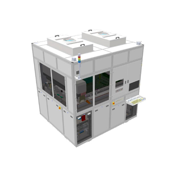
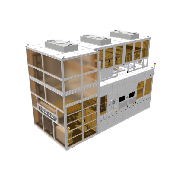
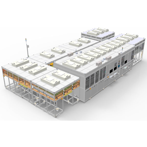
FAVITE’s high-resolution automatic optical inspection (AOI) machine for array processes is specifically designed for array manufacturing. It utilizes a high-speed dynamic optical imaging system and stable image quality hardware design, combined with proprietary detection algorithms, to provide precise defect detection and classification.
Features:
✔ Resolution and defect detection capabilities ranging from 1μm~5μm
✔ Compatible with substrate sizes from G3.5 to G10.5
✔ Zero dead zone detection, achieving 100% coverage of the entire panel area
✔ Superior proprietary image inspection technology supporting all sizes, various pattern designs, and arbitrarily shaped panel products
✔ Intelligent defect classification functionality
✔ Professional and customized services available
Contact
Error: Contact form not found.