Wafer Auto AOI
✔ High-speed line scan inspection + AI defect classification.
✔ Supports front and back surface defect inspection of silicon/glass wafers.
✔ Applicable to CIS/IQC/OQC.
✔ Can be equipped with 8″/12″ EFEM, supports SECS GEM200/300.
Share:
Applied Field
Wafer Inspection
Advanced Packaging
Features
When dealing with wafers of different materials, their chemical and optical properties can directly or indirectly affect the accuracy of image acquisition and defect identification in AOI, and also significantly impact scanning speed.
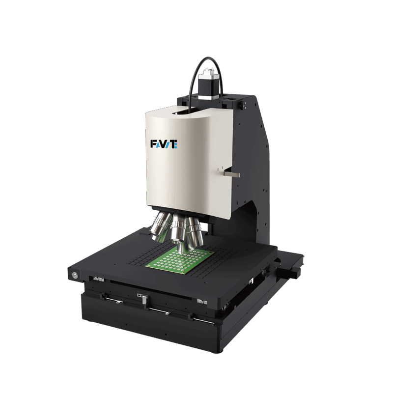
FAVITE’s automated optical defect inspection machine for wafers, equipped with high-speed line scan technology and combined with an AI-powered intelligent defect classification algorithm, can precisely detect various surface defects on both the front and back sides of silicon or glass wafers in a very short time.
Features:
✔ High-speed line scan inspection + AI defect classification.
✔ Supports front and back surface defect inspection of silicon/glass wafers.
✔ Applicable to CIS/IQC/OQC.
✔ Can be equipped with 8″/12″ EFEM, supports SECS GEM200/300.
Contact
Error: Contact form not found.