Wafer Auto AI AOI/OM
✔ Real-time AI defect detection and classification: inspect, capture, and classify instantly.
✔ Can be equipped with 8″/12″ EFEM, supports SECS GEM200/300.
✔ Minimum Detectable Defect Size ≧ 0.3µm
✔ Can be integrated with a yield management system.
Share:
Applied Field
Wafer Inspection
Advanced Packaging
Features
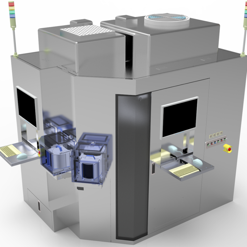
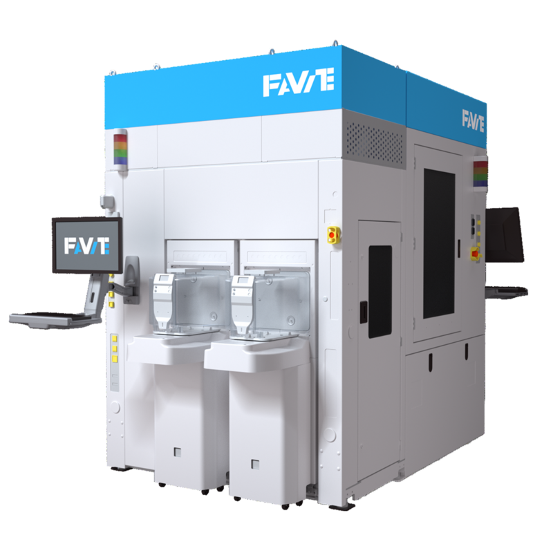
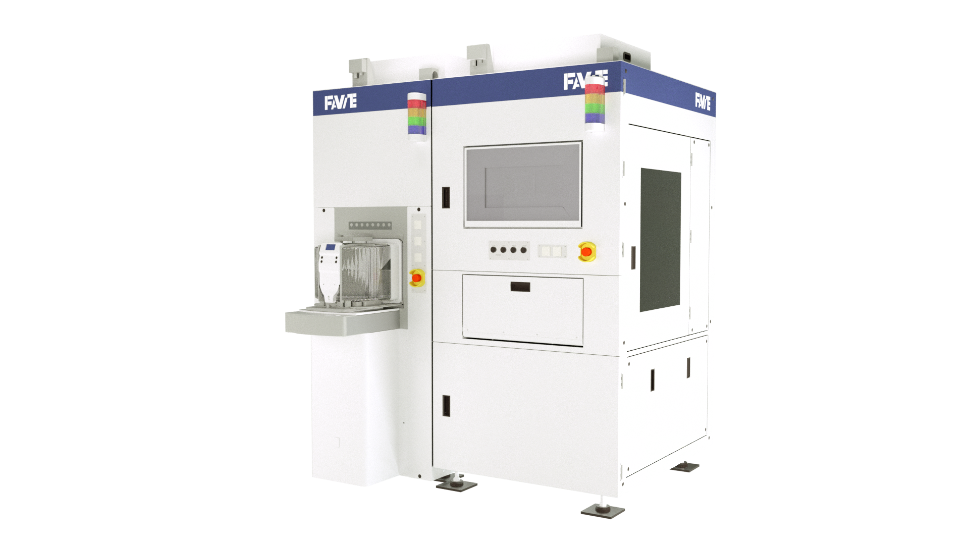
With the increasing complexity and precision of integrated circuits, defects on wafers are not only minute in size but also extremely diverse in type. How to efficiently detect these tiny defects in a short period of time to ensure product quality has become a key success factor for wafer manufacturers.
FAVITE’s automated wafer AI optical review station accurately captures minute defects on wafers through AI defect training and judgment functions. The advantages of immediate inspection, image capture, and classification significantly reduce the time required for inspection.
Features:
✔ Real-time AI defect detection and classification: inspect, capture, and classify instantly.
✔ Can be equipped with 8″/12″ EFEM, supports SECS GEM200/300.
✔ Minimum Detectable Defect Size ≧ 0.3µm
✔ Can be integrated with a yield management system.
Contact
Error: Contact form not found.